
STLINK Programming and Reconfigurable Kit (SPARK)
At a glance
- Status
- Prototype
- Timeline
- May 2025–Present
- Role
- Sole designer — schematic, 4-layer PCB, protection and power architecture, and the fabrication package
- 4-layer PCB on the JLC04161H-7628 stackup, 88.9 mm × 88.9 mm enclosure-driven envelope
- Three independently switched target rails (1.8 V, 3.3 V, 5 V) — default OFF at startup
- SWD, JTAG (10- and 20-pin), UART, SPI, I²C, CAN FD, and GPIO/SWO interfaces
- 22 Ω series resistance and ESD (electrostatic-discharge) protection arrays on every external-facing signal line
- Schematic, 4-layer PCB, ODB++ fabrication package, and BOM in the repository; bench-validation plan defined, not yet executed
Canonical: Source on GitHub — schematic, PCB, fabrication outputs, BOM, validation plan
Overview
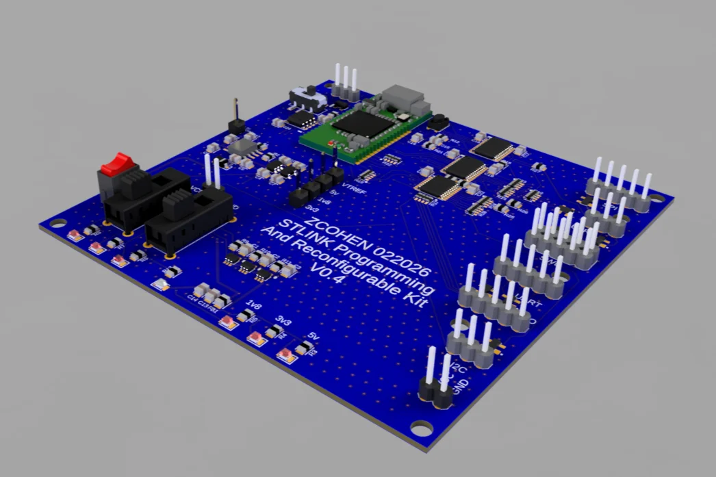
SPARK is a hardened breakout and target-interface board for the STLINK-V3MODS debugger/programmer, built for embedded bring-up in lab and educational environments. The V0.4 architecture emphasizes fault containment, controlled target power distribution, and mixed-signal translation matched to how each bus actually behaves — this is a protection and power-management design, not a passive pin breakout.
Problem
Bare debug probes wired directly to prototype hardware make bring-up fragile: a mis-wired target can back-power the probe, a 5 V line can meet a 1.8 V input, and ambiguous wiring wastes hours of debugging time that has nothing to do with the firmware. SPARK standardizes that interface — protected power entry, target rails that are off until deliberately enabled, translation that respects each signal's electrical behavior, and protection on every line that leaves the board.
Power Architecture
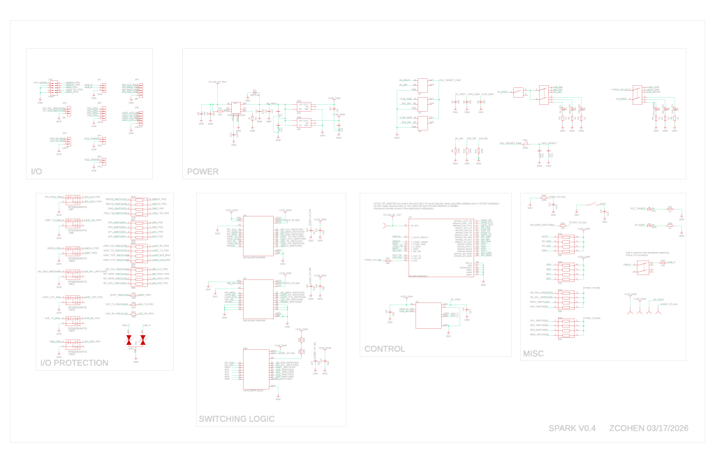
- Protected 5 V entry: the STLINK's 5V_OUT enters through a TPS2596 eFuse before feeding SPARK's master 5 V — overload faults are contained at the entry point, with the eFuse's fault/power-good telemetry available to the design.
- Internal logic rails: dedicated low-noise LDOs generate internal 1.8 V and 3.3 V rails for SPARK's own logic, separate from anything exported to the target.
- Switched target rails:
1.8V_TARGET,3.3V_TARGET, and5V_TARGETare gated by TPS22919 load switches whose enable pins are hardware-pulled down — every target rail defaults OFF at startup and reset, so connecting a board never powers it by surprise. - VTREF policy: target power export and the logic-reference domain are deliberately separate.
5V_TARGETis power only — it is not a claim that the interface I/O is 5 V tolerant — and VTREF is specified at ≤ 3.6 V maximum unless explicit overvoltage protection is added (a documented V1 goal).
Interface and Translation Architecture
SPARK V0.4 uses two translator families, chosen by bus behavior rather than one-size-fits-all:
| Signal / bus | Translator | Why |
|---|---|---|
| I²C | LSF0108 | Open-drain behavior with pull-ups on both sides (SPARK-side pull-ups DNI by default) |
| SWDIO | SN74AXC8T245 | Push-pull path with robust edge control |
| SPI | SN74AXC8T245 | Push-pull / high-bandwidth |
| UART | SN74AXC8T245 | Push-pull / high-bandwidth |
| GPIO / SWO | SN74AXC8T245 | As implemented on push-pull channels |
The CAN interface uses a TCAN1051 CAN FD transceiver with 120 Ω bus termination controlled by a switch, so the board works both mid-bus and at bus ends. The design documentation requires an automotive-rated TVS for the CAN lines' transient environment (part selection remains implementation-dependent).
Protection Strategy
- TPS2596 eFuse on the 5 V entry path
- TPS22919 target-rail gating with default-OFF hardware pulldowns
- 22 Ω series resistance on every external-facing signal line
- SP0503BAHTG ESD arrays on external signals, clamped to ground
Key Design Decisions
- Decision: Gate every target rail through a load switch that defaults off. Rationale: Powering a target should be a deliberate action, not a side effect of plugging in a cable — the safest failure mode for student and lab use.
- Decision: Split translation across LSF0108 and SN74AXC8T245 families. Rationale: Open-drain buses and push-pull buses have opposite electrical needs; a hybrid architecture serves each correctly instead of compromising both.
- Decision: Keep the exported power domain separate from the logic-reference domain. Rationale: The most damaging bring-up mistake is 5 V on a low-voltage pin; the VTREF ≤ 3.6 V policy and power-only 5V_TARGET rail make that mistake structural to avoid.
- Decision: Enclosure-driven 88.9 mm × 88.9 mm board with reinforced mounting. Rationale: The board is lab equipment, not a bare dev board — repeatable mounting and mechanical protection are part of the design.
Implementation & Manufacturing
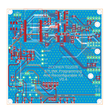
In the repository: the schematic and PCB layout sources, the design archive, an ODB++ fabrication output tree, the master BOM, and CAD board renders. The fabrication output is ODB++ only — RS-274X Gerbers and Excellon drill files are not currently exported. The layout uses heavy ground flooding with via stitching, 12-mil typical routing, and an ENIG finish with ink-plugged vias.
Electronics schematic
PCB layout
No fabrication, assembly, or measurement records are published in the repository. The SPARK repository tracks maturity per stage: Designed and Fabrication package produced are done; Fabricated, Assembled, Electrically verified, and Bench-validated are not. Fabrication receipts, board photos, assembly notes, and measurement records will be added there — and reflected here — as they exist.
Testing & Verification
A bench-validation plan and a first-article bring-up procedure are defined in the repository. They have not been executed and no measurement records are published. Planned V1 hardware goals already identified from design review include a VTREF overvoltage-protection path and an optional split CAN termination network.
When bring-up happens, this section will record what was validated and what needed rework:
- Power entry, eFuse behavior, and switched target-rail validation — pending
- Voltage-domain and level-translation validation (LSF0108 / SN74AXC8T245 paths) — pending
- SWD/JTAG, UART, SPI, and I²C interface validation — pending
- CAN FD transceiver and termination validation — pending
- Protection behavior (series resistance, ESD clamping) — pending
- Discovered problems, rework, and V1 revision changes — documented as found
A real measurement or a documented mistake will carry more weight here than another render; failures and rework will be recorded, not hidden.
Current Status
Prototype. Schematic, 4-layer PCB layout, ODB++ fabrication package, and BOM are complete in the repository. Nothing has been fabricated, assembled, or electrically verified in the repository record. The next milestone is a first-article board and executing the bring-up procedure against it.
Lessons Learned
- Interface hardware earns its complexity: every protective element (eFuse, default-off rails, series resistance) exists because of a specific failure mode seen in real bring-up work.
- Translation architecture is a per-bus decision — treating I²C like SPI is how level shifters end up fighting their own buses.
- Documenting the power policy (what VTREF may be, what 5V_TARGET is not) matters as much as the circuitry, because the interface's users are exactly the people mid-debug.